Description
Detailed Features List
ARMv7 Cortex-A9 CPU(s)
The ARMv7 core supports the following features:
• 88F6810/88F6820/88F6828-Up to 1.866 GHz
• 88F6811/88F6821-Up to 1.33 GHz CPU clock
• 88F6W21-Up to 1.2 GHz CPU clock
• Superscalar RISC CPU with Harvard architecture, variable length, out-of-order pipeline
• NEON SIMD co-processor for improved signal processing
• DSP instructions to boost performance for multimedia and signal processing algorithms
• 32-bit instruction set for high-performance and flexibility
• Thumb-2 and Thumb-EE instruction set for code density
• Single / double precision Floating Point Unit (FPU)
• Symmetrical Multiprocessing (SMP) and Asymmetric Multiprocessing (AMP) modes
• 32-KB L1 Instruction cache 4-way, set-associative, virtually indexed, physically tagged, parity protected
• 32-KB L1 Data cache, 4-way, set-associative, physically indexed, physically tagged, parity protected
• L1 Prefetch:
-- Software driven using ARM PLD instructions
-- Hardware prefetcher that monitors up to 2 data streams
• Table Look-ahead Buffer (TLB):
-- Micro TLB: Two 64-entry fully-associative for Instruction and Data caches
-- Macro TLB: 512-entry 2-way associative structure
• MESI cache coherency scheme
• Hit-under-miss and multiple outstanding requests
• 8-stage pipeline
• Out-of-order execution for increased performance
• Branch Prediction Unit:
-- 2-way Branch Target Address Cache (BTAC) of 4096 entries
-- Global History Buffer (GHB) with 16K 2-bit predictors
-- Return Stack with eight 32-bit entries
• 64-bit internal data bus with 64-bit load / store instructions
• Endianess options-Little or Mixed Endian
• Performance Monitor Unit (PMU) that counts up to 6 event types
• JTAG/ARM-compatible ICE and Embedded Trace Module (ETM) for enhanced real-time debug capabilities
Unified Layer 2 Cache
• 16-way, 1024 KB, write-back and write-through cache
• Physically Indexed Physically Tagged (PIPT)
• Non-blocking pipeline supports multiple outstanding requests and Hit Under Miss(HUM) operation
• Lockdown/way-locking for data and instructions by line or master ID
• Parity protected
DDR3 / DDR3L / DDR4 SDRAM Controller
• 16/32-bit, with an Error-Correcting Code (ECC) option supported by both interface widths
• 88F6810/88F6820/88F6828-Supports DDR3/DDR3L-1600/1866 and DDR4-1800
• 88F6811/88F6821-Supports DDR3/DDR3L-1333
• 88F6W21-Supports DDR3/DDR3L-1200
• Supports synchronous clock ratio of 1:N and 2:N between the CPU cores and the DRAM interface
• Supports asynchronous clock frequencies between the CPU cores and the DRAM interface
• Supports 1.5 and 1.35V for DDR3 (SSTL) and 1.2V for DDR4 (POD1)
• Smart scheduler for transaction re-ordering and QoS
• Auto calibration of I/O output impedance
• Up to 8 Gb for DDR3 and 16 Gb for DDR4 (supports all DDR devices densities, according to the JEDEC standard)
• DDR3/DDR4 write and read leveling support
• Proprietary data and control eye pattern optimization process to improve signal integrity
• DDR3 address mirroring support
• Supports DDR3/DDR4 BL8
• Supports the 2T and 3T modes to enable high-frequency operation even under a heavy-load configuration
• Supports SDRAM bank interleaving
• 8/16 open pages per rank (DDR3 and DDR4, respectively)
• Up to a 128-byte burst per single memory
• Supports x8 and x16 memory devices
• Supports the following DDR4 features:
-- DDR4 PDA (Per DRAM Accessibility)
-- DDR4 MRS readout
-- DDR4 different bank group timings
-- Supports different pin mapping for DDR3/DDR4 optimization of board routing
Gigabit Ethernet (GbE) Ports
• 88F6810
-- 2 GbE ports (0 and 1)
-- SGMII / RGMII / MII interface
• 88F6820/88F6828
-- 3 GbE ports (0-2)
-- SGMII / QSGMII / RGMII / MII interface
• 88F6811/88F6821/88F6W21
-- 2 GbE ports (0 and 1)
-- SGMII / RGMII / MII interface
• SGMII supports 10/100/1000/2500 Mbps
• Full-wire speed receive and transmit of short packets
• Support for IEEE 1588v2 (PTP)
• DA filtering
• Strict priority/WRR arbitration between 8 transmit queues with rate limiting
• Per queue egress rate shaping
• Support for queuing based on Marvell® DSA tag
• Support for jumbo frames (up to 10K) on both receive and transmit
• TCP/IP checksum acceleration
• Support for IEEE 802.3az (Energy-Efficient-Ethernet)
• Support for Wake-On-LAN
Hardware Buffer Management
• 4 independent buffer pools
• Up to 64 KB elements per pool
• Dedicated DMA engines for read-ahead or write-back from/to external memory
PCI Express (PCIe) Interface
• 88F6810/88F6811/88F6821-Supports 3 ports x1 lanes
• 88F6W21-Supports 2 ports x1 lanes
• 88F6820/88F6828-Supports 1 port x4 lanes and additional 2 ports x1 lane or up to 4 ports x1 lane
• PCIe Gen 1.1 at 2.5 Gbps / Gen 2.0 at 5 Gbps signaling
• Supports Root Complex and Endpoint modes
• Lane polarity inversion/reversal support
• Maximum payload size of 128 bytes
• Single Virtual Channel (VC-0)
• Replay buffer support
• Extended PCIe configuration space
• Power management: L0s and L1 ASPM active power state support; software L1 and L2 support
• Error message support
• PCIe master specific features:
-- Host to PCIe bridge-translates CPU cycles to the PCIe memory or configuration cycles
-- Supports DMA bursts between memory and PCIe
-- Supports up to 4 outstanding read transactions
-- Maximum read request of up to 128 bytes
• PCIe target specific features:
-- Supports reception of up to 8 read requests
-- Maximum read request of up to 4 KB
-- Supports PCIe access to the device internal and external space
High-Speed Integrated SERDES Lanes
• 88F6810-Integrates 5 low-power, high-speed SERDES PHYs, based on proven Marvell SERDES technology
• 88F6811/88F6821/88F6W21-Integrates 4 low-power, high-speed SERDES PHYs, based on proven Marvell SERDES technology
• 88F6820/88F6828-Integrates 6 low-power, high-speed SERDES PHYs, based on proven Marvell SERDES technology
• Diverse multiplexing options of PCIe, SATA 3.0, SGMII, QSGMII, and USB 3.0 interfaces
USB Controllers
• 88F6810/88F6820/88F6828-3 USB ports configurable from the following 4 USBcontrollers:
-- 2 USB 3.0/2.0 Host compliant ports with integrated PHYs
-- 1 USB 3.0 Device compliant port with integrated PHYs
-- 1 USB 2.0 Host or Device compliant port with integrated PHY
• 88F6811/88F6821-2 USB ports configurable from the following 3 USB controllers:
-- 2 USB 3.0/2.0 Host compliant ports with integrated PHYs
-- 88F6811/88F6821-1 USB 3.0 Device compliant port with integrated PHYs
• As a Host:
-- Extensible Host Controller interface (xHCI) compatible
-- Supports direct connection to all device types (SS, HS, FS, LS)
-- Supports up to 64/16 independent endpoints (USB 3.0/USB 2.0, respectively)
• As a Device:
-- Connects to all host types (SS, HS, FS) and hubs
-- Supports up to 16/4 independent endpoints (USB 3.0/USB 2.0, respectively)
• Supports control, interrupt, bulk, and isochronous data transfers
• USB Power Management states:
-- U0 (Active), U1 (Idle), U2 (Deep Idle), and U3 (Suspended) for USB 3.0
-- Suspend and Resume for USB 2.0
2 Marvell® 6 Gbps (Gen 3x) SATA 3.0 Ports
• 88F6810/88F6820-2 fully compliant SATA 3.0 ports
• 88F6828-4 fully compliant SATA 3.0 ports
• 88F6811/88F6821-2 fully compliant SATA 3.0 ports
• 88F6W21-1 fully compliant SATA 3.0 port
• Supports communications speeds of 6.0 Gbps, 3.0 Gbps, and 1.5 Gbps
• Supports Gen 1x, Gen 2x, Gen 3
• Supports programmable transmitter signal levels
• Supports Native Command Queuing (NCQ) and First Party DMA (FPDAM) with up to 32 outstanding commands per port
• Supports AHCI 1.0 and IDE programming interfaces
• Supports Port Multiplier (PM)-Performs FIS-Based-Switching as defined in the SATA working group PM definition
• Port Selector (PS)-Issues the protocol-based Out-of-Band (OOB) sequence to select the active host port
• Supports external SATA (eSATA)
• Supports Partial and Slumber power management states
• Advanced interrupt coalescing
• Advanced drive diagnostics via the ATA SMART command
2 Cryptographic Engines
• Hardware implementation on Encryption/Decryption and Authentication engines to boost IP security (IPsec) and file encryption/decryption
• Dedicated DMA to feed the hardware engine with data from the internal SRAM memory or from the DDR memory
• Implements AES, DES, and 3DES encryption algorithms
• Implements SHA2, SHA1, and MD5 authentication algorithms
4 XOR DMA Engines
• RAID5 P (XOR parity) generate and repair up to 8 source blocks
• RAID6 P and Q generate and repair up to 8 source blocks
• Memory copy (DMA) acceleration
• iSCSI CRC-32 calculation
• Memory initialization function
TDM Controller
• Supports 2 independent VoIP channels
• Generic interface to standard SLIC / SLAC / DAA / codec devices
• Compatible with standard PCM highway formats
• Supports various bit clock rates (256 kHz to 8.192 MHz, in increments of powers of 2)
I2S Input/Output and S/PDIF Output Audio Interfaces
• Sample rates of: 44.1, 48, and 96 kHz
• Compliant with IEC 60958-1, 60958-3, and 61937 specifications
• Supports plain I2S, right-justified, and left-justified formats
Device Bus Controller
• 8/16-bit multiplexed address / data bus
• Supports different types of standard memory devices, such as NOR Flash and ROM
• Up to 5 chip selects with programmable timing
NAND Flash Controller
• Native support for NAND Flash with up to:
-- 8 KB page size
-- 16-bit ECC per page
• 4 chip selects with programmable timing and optional external wait-state control
2 SPI Ports
• General purpose 1-bit SPI interface
• SPI port has up to 4 chip selects
SD / SDIO / MMC / eMMC Host Interface
• 1-bit / 4-bit SDmem, SDIO 3.0
• 1-bit / 4-bit / 8-bit MMC 4.4 for eMMC
• SDR-50: Up to 100 MHz
• HS-DDR: Up to 50 MHz
• Hardware generate/check CRC on all command and data transactions on the card bus
2 UART Interfaces
• 16750 UART compatible
• Each port has:
-- 2 pins for transmit and receive operations
-- 2 pins for modem control functions
Advanced Power Management
• CPU Power Management states:
-- Deep Idle (CPU power down)
-- Idle (CPU clock gating)
-- Throttle (CPU reduced speed)
-- Run (CPU full speed)
• Standby with Real Time Clock (RTC) alarm or external wake-up options
• Wake-On-LAN (WOL) with lossless packet reception
• SDRAM Self Refresh and Power Down modes
• Selectable clock gating of different interfaces
• PCIe, SGMII, USB, and SATA SERDES shutdown
• Energy Efficient Ethernet (EEE)
• Various wake-up options
2 I2C Interfaces
• General purpose I2C master/slave ports
• EEPROM Serial initialization support
Real Time Clock
• External system wake-up
• Battery backup
Integrated BootROM
• Boot from Flash (SPI, parallel NOR, parallel NAND, serial NAND (SPI-NAND), and SDIO / MMC / eMMC)
• Boot from PCIe or SATA
• Secured boot flow
2 Integrated Low Drop Out (LDO) Controller
• On-chip LDO controller for external Positive-Negative-Positive (PNP) transistors
• Programmable output voltages of 1.8/2.5V with 50 mV resolution.
Multi-Purpose Pins (MPP)
• 88F6810/88F6820/88F6828-60 MPP pins dedicated for peripheral functions and General Purpose I/O (GPIO)
• 88F6811/88F6W21/88F6821-48 MPP pins dedicated for peripheral functions and General Purpose I/O (GPIO)
• Each pin independently configurable
• GPIO inputs configurable to register interrupts from external devices and generate maskable interrupts
• GPIO outputs configurable for PWM control of LED or fan operation
Clock Generation
• Internal generation of CPU clock, Core clock, SDRAM clock, RGMII/MII clock, SERDES clock, TDM clock, Audio clock, and external Reference clock from a single 25-MHz reference clock
• Supports internal generation of spread spectrum clocking on the CPU subsystem and SDRAM interface
Interrupts
ARM compliant Generic Interrupt Controller (GIC), version 1
Thermal Sensor
On-die Thermal Sensor with over-heat interrupt
Timers/Counters and Watchdog Timers
Integrated programmable 32/64-bit timers/counters and watchdog timers
Package
88F6810/88F6820/88F6828-TFBGA 17x17 mm package, 0.8 mm ball pitch
88F6811/88F6821/88F6W21-TFBGA 14x14 mm package, 0.65 mm ball pitch
Marvell Technology, Inc. is an American company, headquartered in Santa Clara, California, which develops and produces semiconductors and related technology. Founded in 1995, the company had more than 6,000 employees as of 2021, with over 10,000 patents worldwide, and an annual revenue of $4.5 billion for 2021.
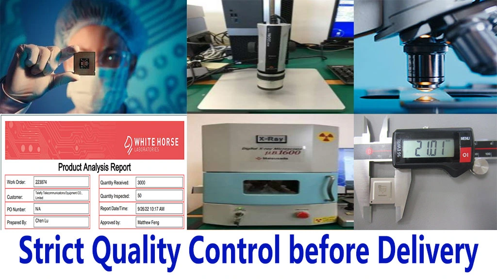
2. All products we provide will be double checked and proper inspection process will be strictly followed before delivery.
3. We promise to provide at least 1 year after-sell service for all products we sell.
4. Due to the reality of sometime volatile changes of the chips and components' stock and prices, please contact with us for their availability and quoting prices before payment.
5. We use DHL, UPS, FedEx, TNT, HONGKONG Post, EUB, EMS or other global express delivery services you designate. Company Profile
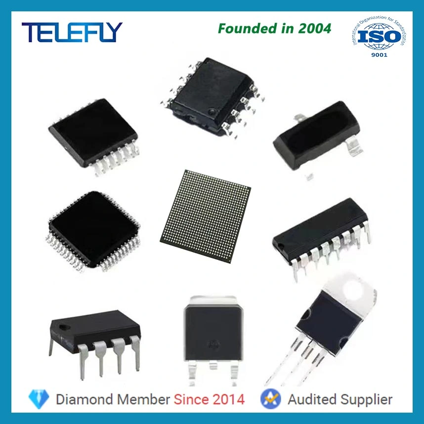
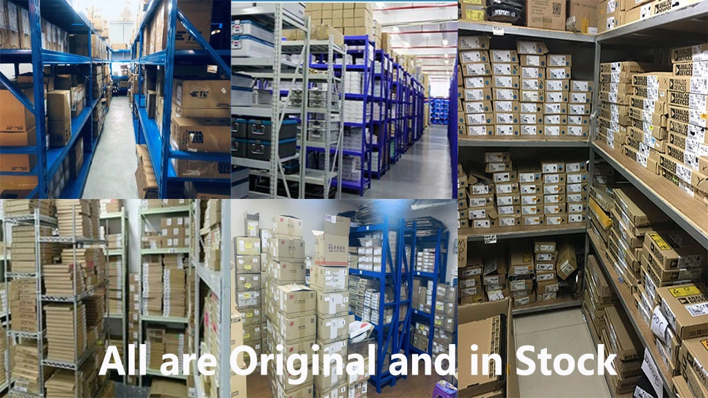
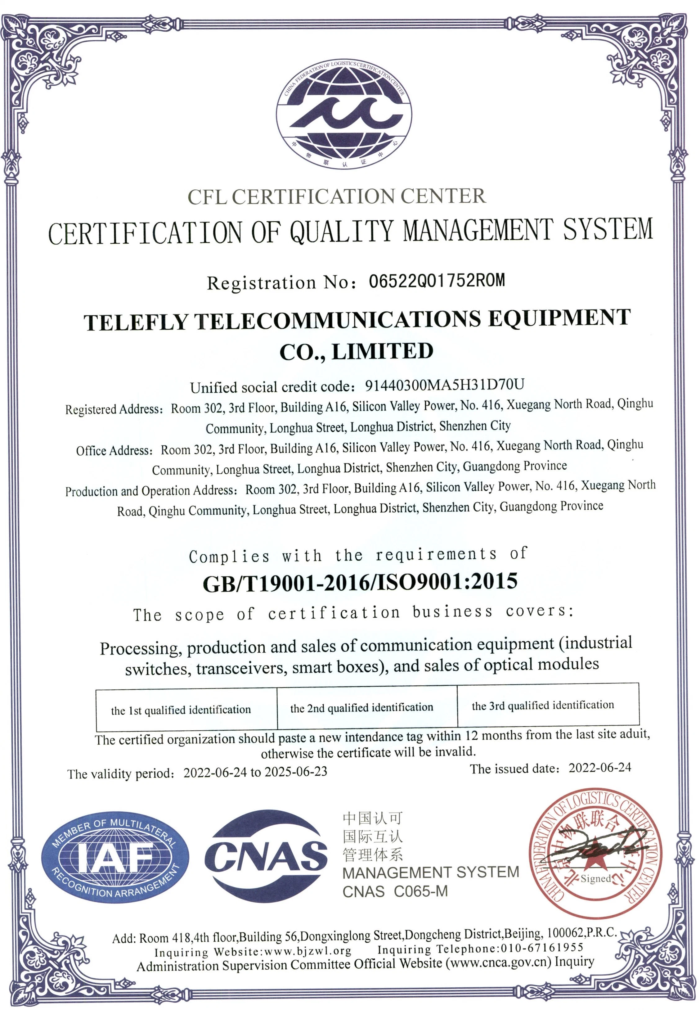
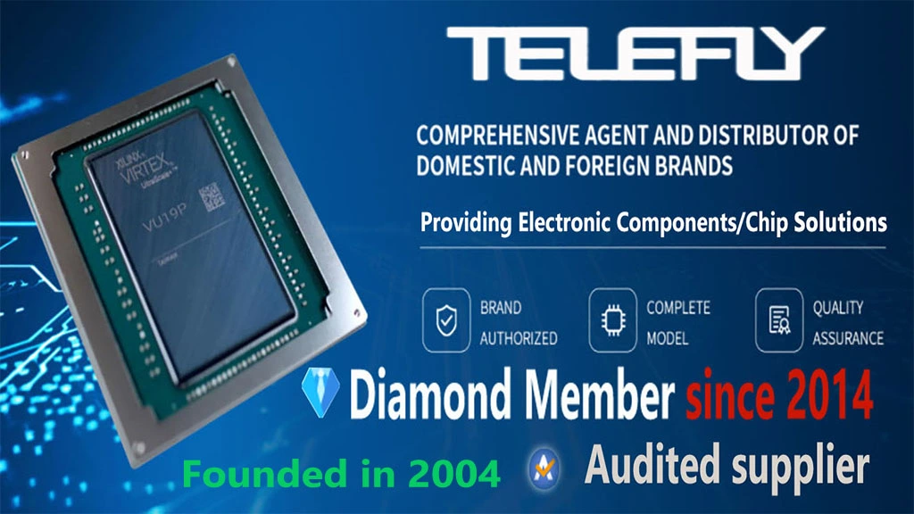
Company ProfileTELEFLY Telecommunications Equipment Co., Ltd. is a leading Chinese Telecommunications Equipment manufacturer and a semiconductor chip and other electronic component distributor founded in 2004, certified by SGS, CFL Certification Center. We provide high quality and price competitive semiconductor chips and other electronic components, Ethernet switch ,SFP transceiver,media converter ,patch cable, Fiber Optic Splitter and so on. Up till now, our products and solutions have been deployed in over 60 countries and regions, TELEFLY is looking forward to strengthening friendly cooperative relationships with all clients, creating benefits together and sharing the joy of success!Our Advantages
Why you choose TELEFLY be one of your partner?
1.Customer get satisfied quality and service with competitive price and punctual delivery.
2.OEM service with 13-year experiences, free samples are available.
3.Prompt answer for any question and inquiry in the shortest time.
4.Factory directly,reduce your cost and save time.
1.Customer get satisfied quality and service with competitive price and punctual delivery.
2.OEM service with 13-year experiences, free samples are available.
3.Prompt answer for any question and inquiry in the shortest time.
4.Factory directly,reduce your cost and save time.FAQ
Q1 . What your MOQ?
A1 .If not specified, 1 pcs is ok,whatever how many you need,and we will also give you the best service.
Q2.What certification did you get?
A2 : Our product strictly operate the ISO9001:2008 quality control system and we passed the CE,FCC,ROHS and SGS test,you can trust us.
Q3 :What about your package and delivery,will it broke during shipping?
A3:You don't need to worry about the package,we will use shockproof case for delivering.
Q4.What your common delivery way?
A4:By air, by sea or express(UPS,DHL,Fedex,TNT,EMS...)We will make a perfect delivery plan for you.
Q5.Tell me some detail about warrant time.
A5:We give you the promise if any question during 1 year and not cause by human factors,we will fix it.

 Complaint